| TA2020 Digital Amplifier |
At last I ate a forbidden fruit. In these 5 years I have been convinced that I am one of the analog factions who often make the vacuum tube amplifiers. I found many web sites where various cheap digital amplifier kits are introduced. Therefore I bought "TA2020-020 Digital Amplifier Complete Kit" of Wakamatsu for the first trial.
About 3 days was necessary for boring holes in the case, installing of all parts to the case, and inside wiring. It is said that the interference with AM radio will occur because of the high frequency for digital amplification. But in reality any noise did not occur. The cost performance of digital amplifier seems considerably high.
 The picture shows a general principle of digital amplification. The audio signal of 20Hz to 20kHz is
pulse-width modulated by a carrier wave of 100kHz to 1MHz. The modulated wave is amplified by the switching FET.
The original audio signal is regenerated through the low pass filter composed of LC circuit.
The maximum output power depends on the power supply voltage because the work of FET is only on-off switching.
The picture shows a general principle of digital amplification. The audio signal of 20Hz to 20kHz is
pulse-width modulated by a carrier wave of 100kHz to 1MHz. The modulated wave is amplified by the switching FET.
The original audio signal is regenerated through the low pass filter composed of LC circuit.
The maximum output power depends on the power supply voltage because the work of FET is only on-off switching.
According to the brochure of Tripath, the frequency of carrier wave alters between 100kHz and 1MHz depending on that of original audio signal. This is an application of the spread spectram technology and works to suppress the residual carrier component in the output of digital amplifier.
If you put the mouse over the image, it will be
enlarged. (Same below)
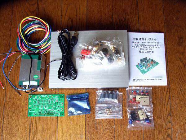 All parts of the complete kit are shown. They are: IC base of TA2020-020 digital amplifier,
case, inverter type power supply with DC 12V 50W, variable resistor, speaker terminal, RCA jack, LED diode,
power switch, shield wire, and connection wire.
All parts of the complete kit are shown. They are: IC base of TA2020-020 digital amplifier,
case, inverter type power supply with DC 12V 50W, variable resistor, speaker terminal, RCA jack, LED diode,
power switch, shield wire, and connection wire.
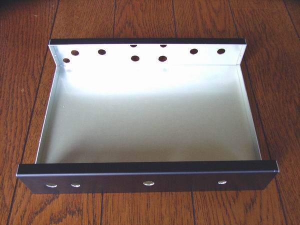 This is the case after boring of necessary holes. The dimension of the case is: 200 (W) x 150 (D) x 40 (H) mm.
 This is the case after installing of power supply inverter and main parts.
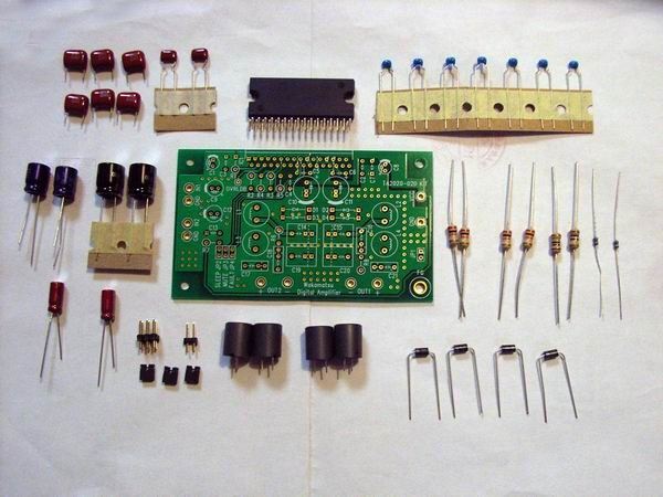 The picture shows all parts for digital IC base which are composed of the base, IC, resistors, condensers,
coils, diodes, shorting bars, etc.
The major technical specifications of Tripath Digital IC are as follows:
The picture shows all parts for digital IC base which are composed of the base, IC, resistors, condensers,
coils, diodes, shorting bars, etc.
The major technical specifications of Tripath Digital IC are as follows:
Power supply voltage: DC 8.5V - 14.6V
Output power: 20W at 13.5V 4ohms, 10W at 13.5V 8ohms
Distortion rate: 0.03% THD+N at 10W 4ohms, 10% THD+N 22W 4ohms
Channel separation: -80dB at 1kHz
Idling current: 64mA
Power efficiency: 88% at 12W 8ohms
 This is the digital amplifier base completed. It required about an hour for soldering.
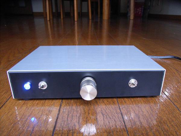 This is the front view of digital amplifier. The volume controller is located at the center, input switch at
the right, power switch and blue LED diode at the left.
The kit originally has only one pair of input jack, therefore I added another pair for switching
of CD and Tuner.
This is the front view of digital amplifier. The volume controller is located at the center, input switch at
the right, power switch and blue LED diode at the left.
The kit originally has only one pair of input jack, therefore I added another pair for switching
of CD and Tuner.
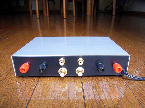 A rear view of digital amplifier is shown. There are different type of RCA jacks because
I could not buy the same type of RCA jack.
A rear view of digital amplifier is shown. There are different type of RCA jacks because
I could not buy the same type of RCA jack.
 The picture shows the inside of digital amplifier. There is not heat sink for the amplification IC.
In order to cancel the pop noise at the time of power supply injection, a delay connection of the speaker
circuit is made by a small relay "G6A-274P" of Omron.
Although the maximum point-of-contact current is 2 amperes, since it uses by the small power which is usually
about 1W to 2W, I think it is satisfactory.
The picture shows the inside of digital amplifier. There is not heat sink for the amplification IC.
In order to cancel the pop noise at the time of power supply injection, a delay connection of the speaker
circuit is made by a small relay "G6A-274P" of Omron.
Although the maximum point-of-contact current is 2 amperes, since it uses by the small power which is usually
about 1W to 2W, I think it is satisfactory.
 The picture shows the circuit diagram of digital amplifier. The part with red color was newly added to
the complete kit. Two electrolysis condensers of 16V 10000μF and 16V 2200μF were added to reinforce
power supply circuit. The input circuit was improved from single to double. In order to eliminate the
big pop noise at the time of power supply injection, a time delay circuit for about 5 seconds was equipped
between the amplifier and the speaker terminal.
The picture shows the circuit diagram of digital amplifier. The part with red color was newly added to
the complete kit. Two electrolysis condensers of 16V 10000μF and 16V 2200μF were added to reinforce
power supply circuit. The input circuit was improved from single to double. In order to eliminate the
big pop noise at the time of power supply injection, a time delay circuit for about 5 seconds was equipped
between the amplifier and the speaker terminal.
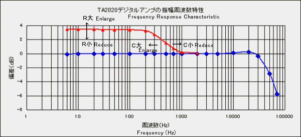
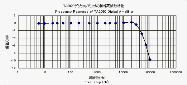 The frequency response curve in case of load resistance of 4ohms is shown. Especially it is
excellent in low frequency. The residual noise level is 1.2mV and the damping factor at 1kHz is 9.1.
The frequency response curve in case of load resistance of 4ohms is shown. Especially it is
excellent in low frequency. The residual noise level is 1.2mV and the damping factor at 1kHz is 9.1.
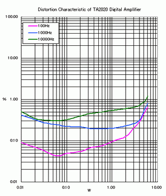 This is the distortion characteristic of the digital amplifier.
These curves are somewhat mysterious, that is, the distortion rate of 100Hz is better than that of 1kHz or 10kHz.
I used a PC software (WaveSpectra) to measure the distortion rate, but it was difficult to measure it due
to the fluctuation of each spectrum level.
Since the gain of amplifier is small, more than 6W of the output power could not be obtained with the
signal generator by a CD player.
However the distortion rate is less than 1% until the output power reaches 6W.
This is the distortion characteristic of the digital amplifier.
These curves are somewhat mysterious, that is, the distortion rate of 100Hz is better than that of 1kHz or 10kHz.
I used a PC software (WaveSpectra) to measure the distortion rate, but it was difficult to measure it due
to the fluctuation of each spectrum level.
Since the gain of amplifier is small, more than 6W of the output power could not be obtained with the
signal generator by a CD player.
However the distortion rate is less than 1% until the output power reaches 6W.
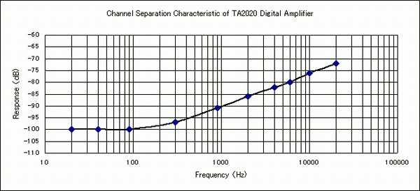 This is the channel separation characteristic of the digital amplifier.
The curve becomes bad in high frequency, but is very good in low and middle frequency.
Especially in very low frequency, the channel separation is as good as -100dB, which is excellent in
comparison with the single vacuum tube amplifier.
This is the channel separation characteristic of the digital amplifier.
The curve becomes bad in high frequency, but is very good in low and middle frequency.
Especially in very low frequency, the channel separation is as good as -100dB, which is excellent in
comparison with the single vacuum tube amplifier.
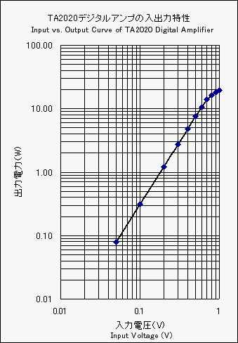 The input vs. output charasteristic curve in case of load resistance of 4ohms is shown.
It seems the maximum output power is about 15W. The overall voltage gain is 11 times.
The input vs. output charasteristic curve in case of load resistance of 4ohms is shown.
It seems the maximum output power is about 15W. The overall voltage gain is 11 times.
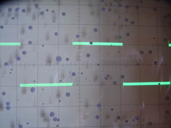
 The residual carrier component in case of no input signal with maximum gain is shown. Its
frequency is 800kHz with a voltage level of 100mVp-p. There is not at all the sense of incongruity when
I hear the sound. Any interference with AM radio does not occur due to the excellent technology of
spread spectrum and inverter type power supply.
The residual carrier component in case of no input signal with maximum gain is shown. Its
frequency is 800kHz with a voltage level of 100mVp-p. There is not at all the sense of incongruity when
I hear the sound. Any interference with AM radio does not occur due to the excellent technology of
spread spectrum and inverter type power supply.
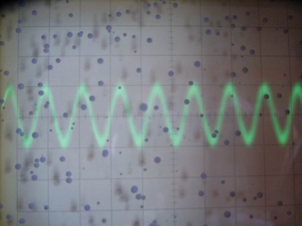
 1kHz sine wave form of output at the level of 2Vp-p is shown. A little carrier component
overlaps on the audio signal.
1kHz sine wave form of output at the level of 2Vp-p is shown. A little carrier component
overlaps on the audio signal.
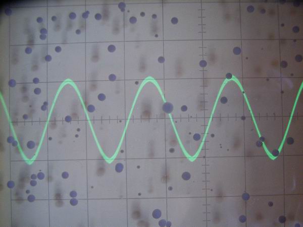
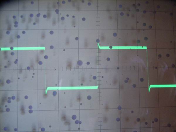
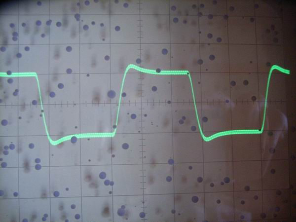
 The responses of square wave form at the level of 2Vp-p are shown, from the top, 100Hz,
1kHz and 10 kHz. A small quantity of overshoot and residual carrier component overlapped on the respective
square wave is seen.
The responses of square wave form at the level of 2Vp-p are shown, from the top, 100Hz,
1kHz and 10 kHz. A small quantity of overshoot and residual carrier component overlapped on the respective
square wave is seen.
The following is my impression after making a digital amplifier with lower cost than vacuum
tube amplifier:
1. A good sound comes out but nobody notices that it is the sound of digital amplifier.
2. It produces very little heat, therefore is recommendable as one of anti-global warming measures.
3. It does not produce high frequency noise which interferes with AM radio.
4. Because there is no adjustment point, it is easy to make it.
5. It can be made smaller in comparison with the large output power.
6. Because the power supply is unipolar, it can be made easily with lower cost.
7. A big pop noise comes out when the power is on but this can be eliminated by a time delay circuit.
Subsequent modification: Application of bass boost cuircuit
 I applied a bass boost circuit later on to improve low frequency characteristic for BOSE 101MM small size
speaker. Two sets of elements (10k ohom and 0.033μF) were added in operational amplifier.
I applied a bass boost circuit later on to improve low frequency characteristic for BOSE 101MM small size
speaker. Two sets of elements (10k ohom and 0.033μF) were added in operational amplifier.
 The low frequency characteristic using the bass boost circuit is shown. About 3.5 dB at the very low
frequency was improved.
The low frequency characteristic using the bass boost circuit is shown. About 3.5 dB at the very low
frequency was improved.